
Infineon puts working power devices on a 300 mm SiC wafer—but gives no production date
Infineon says it fabricated functional silicon-carbide power devices on a 300 mm wafer using an established fab and existing silicon equipment. The larger format could improve throughput, but the company disclosed no yield, reliability data or schedule for volume production.
The story
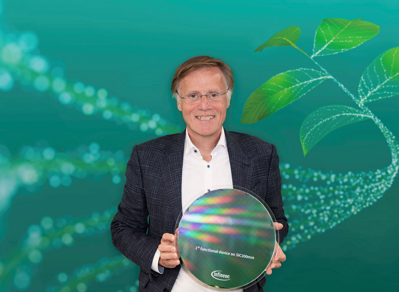
Infineon Technologies says it has fabricated functional power devices on a 300-millimeter silicon-carbide wafer at its semiconductor plant in Villach, Austria. Announced on November 9, the demonstration used existing silicon manufacturing equipment in a full-scale fab environment. It is a meaningful step toward putting SiC power electronics onto the wafer format already standard across much of advanced silicon manufacturing—but it is not yet a production announcement.
The wording matters because 300 mm SiC is no longer synonymous with a single first. Wolfspeed announced in January that it had produced a single-crystal 300 mm SiC wafer. Infineon's narrower claim is that it processed a wafer of that diameter into working power devices inside an established semiconductor fab. The company plans to display the processed wafer at electronica in Munich from November 10 to 13. It did not identify the device type or publish electrical results.
Moving from 200 mm to 300 mm expands the wafer area by 2.25 times. Infineon says the larger format can provide about 2.3 times as many chips per wafer, which is geometrically plausible before edge effects and yield are counted. A fabrication cycle can therefore spread tool time and other fixed costs over more dies. But wafer diameter does not improve a transistor's electrical performance by itself, and a larger surface can magnify the economic damage from crystal defects or non-uniform processing.
Silicon carbide earns the effort because it can switch high voltages with lower losses and operate at higher temperatures than conventional silicon in many power applications. Those traits support smaller, more efficient traction inverters, chargers, renewable-energy converters, industrial drives and data-center power systems. The cost and availability of qualified devices, however, still limit wider adoption. Larger wafers are one possible route to better manufacturing economics, not a guarantee of them.
Independent technical reporting by Electronic Design highlights what remains undisclosed. Infineon supplied no device specifications, manufacturing yields, wafer maps or schedule for volume output. The company also did not say which silicon tools were reused or what modifications they required. SiC processing includes demanding steps—such as very high-temperature dopant activation and careful gate-oxide formation—that do not map automatically onto a silicon production line. Maintaining flatness, stress control and uniform electrical behavior across 300 mm is part of the challenge.
Infineon paired the device announcement with a substrate-processing claim. At its Dresden site, it says it demonstrated its Cold Split method on 300 mm SiC. The laser-based process creates a controlled separation plane so a wafer can be removed from a crystal boule with less material loss than conventional wire sawing. Because SiC crystal is expensive and difficult to grow, reducing kerf loss could matter as much as fitting more dies onto each wafer. Infineon disclosed no recovery rate, surface-quality result or throughput figure for the 300 mm trial.
The company is therefore running two linked experiments: whether large SiC substrates can be separated efficiently, and whether they can pass through enough of an existing 300 mm tool chain to make functional devices. That integration may lower future capital requirements by reusing proven automation and metrology. Yet commercial economics depend on the steps that a demonstration does not reveal: repeatability across many wafers, acceptable die yield, reliability qualification and the cost of specialized SiC operations that cannot reuse silicon tools.
INNOVOX analysis: Infineon's result moves 300 mm SiC from a materials milestone toward a manufacturing-system milestone. That is consequential because power semiconductors are becoming infrastructure for electrification and AI, not only components inside electric cars. A credible 300 mm route could eventually expand supply and reduce cost per good die. The strongest signal today is organizational: Infineon can coordinate crystal handling, device processing and fab automation at this scale. The weakest signal is economic, because none of the numbers needed to prove an advantage has been published.
What to watch next is evidence rather than another diameter record. Useful disclosures would include breakdown voltage, on-resistance and leakage distributions across multiple wafers; defect density and usable-die yield; reliability testing; customer sampling; and a firm ramp schedule. Infineon says it will plan timing with customers while continuing its 200 mm SiC roadmap. Until those data arrive, the 300 mm wafer should be treated as a technically credible bridge to industrialization—not proof that mass-produced SiC devices are about to become cheaper.
INNOVOX analysis
The milestone is best read as a manufacturing-integration proof, not a cost breakthrough. Infineon has shown that functional SiC devices can emerge from a 300 mm flow in an established fab. The commercial prize comes only if crystal quality, wafer flatness, process uniformity and reliability survive at production yield.
What to watch
Watch for electrical distributions across multiple wafers, defect and usable-die yields, automotive or industrial qualification, customer samples, and a disclosed ramp date. Also watch whether Infineon's 300 mm Cold Split process measurably reduces substrate loss and cost.